Measuring Lasers Used in Photovoltaic Solar Panel Manufacturing

One of the recent developments in the photonics industry has been the rapid increase in automated solar panel production facilities. Many of these end-to-end production lines use laser-based methods to manufacture the thin film silicon photovoltaic modules. The lasers used for this activity are generally diode-pumped solid-state lasers at 1064 nm, 532 nm and 355 nm with beams focused to around 30 μm. They are run at powers or energies that, although not extremely high, have high power or energy densities at these small beam diameters. The techniques used often call for multiple beams, running in parallel, to make precise cuts to electrically isolate the sections of the photovoltaic sheets. To ensure that these cuts are uniform, it is important to measure the beam profiles.

Measuring the profile of a high power density beam with a small diameter can be tricky. Cameras are not very good at measuring beams with diameters of less than 50μm, and the attenuation required for the high power or energy densities can be substantial. The attenuationf can also be a source of beam distortion, which adds great uncertainty to the data. Proper attenuation of high power beams can be quite complex and generally requires multiple levels of attenuation provided by both reflective and absorptive filters. The first stages of attenuation need to be reflective attenuators, which in turn generate additional beams (reflections) that must be controlled or captured with beam dumps. It is not unusual to need four to six stages of attenuation to get a beam power to the level necessary to make camera measurements. It can be difficult to find space for this in the solar panel production modules.

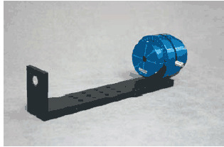
In concert with several of the companies building photovoltaic manufacturing equipment, Photon has developed measurement instruments that are uniquely suited to making these measurements. The NanoScan slit-based profiler has the capability of measuring small beams directly with little or no attenuation, making it a logical choice for these types of analyses. However, some of these beams are operated as pulsed beams, which complicate the measurement somewhat. Although the NanoScan is capable of measuring pulsed beams, small diameter beams present a problem. Unless the repetition frequency of the pulses is very high, the nature of pulsed beam analysis limits the size that can accurately be measured.4 In addition, as the beam’s diameter decreases, the power or energy density increases dramatically, making damage to the profiler a possibility. By using a simple magnification system, it is possible to make direct measurements of the beams. Photon has coupled a high power 10x objective into the NanoScan Near-Field Profiler system to create an instrument specifically designed to measure the typical laser output used in the solar panel manufacturing process. Expanding the beam 10-fold reduces the power or energy density by two orders of magnitude (1/100). It also makes the measurement of pulsed beams ossible at lower repetition rates. The minimum beam diameter that can be measured with the NanoScan for a 20 kHz pulsed laser is ~90μm—well above the 30μm beam size required for this application.5 Expanding the beam to 300μm makes it easy to measure at this pulse frequency.

Near Field Profiler with NanoScan and high power asphere lens

In order to make accurate measurements with this system it is necessary to calibrate the actual magnification of the lens. This can easily be accomplished by using a precision stage to translate a source a known distance and measuring the motion recorded by the NanoScan. For example if moving the source 100μm, shows a motion on the NanoScan of 987μm, then the actual magnification factor of the entire set up is 9.87X. This value can then be entered into the NanoScan software as the magnification factor. The NanoScan will then report the actual value of beam size and pointing measurements.

Some users may choose to make direct measurements of the beams in order to ensure that there are no additional variables introduced into the measurements from the instrument optics. The NanoScan is still the best instrument to make these measurements because it can handle considerable power and is capable of accurately measuring the small beam diameters found in the solar panel applications. It is necessary to exercise caution to be sure that the power or energy densities stay below the damage thresholds of the NanoScan slits. Photon can provide detailed information to allow the customer to determine these levels for both CW and pulsed beams. The slit damage calculator6 will provide a convenient method to determine these limits.

Either way that is chosen to measure the beams used for solar panel production, directly or with magnification, Photon has the tools and the knowhow to create a system that will provide reliable, accurate and efficient measurements. Photon NanoScans are calibrated to NIST Traceable standard, so there is no doubt that the measurements are reflecting the reality of the laser performance.

References

  1. Photonics Spectra, Photonics Technology News, September 2008
  2. www.photonics.com “Solar Photonics: Lasers support Emerging Solar Industry Needs”
  3. Lasers that are operated in pulsed mode are measured in energy per pulse (Joules); continuous wave lasers in average power (Watts).
  4. For additional explanation of the relationship between beams size and pulse frequency refer to the Application Note entitled “Measuring Pulsed Beams with a Slit Based Profiler,” available from Photon Inc at www.photon-inc.com
  5. Application Note “ Measuring Pulsed Beams with a Slit Based Profiler”
  6. The Slit Damage Calculator is an Excel® spread sheet that is available on line at www.photon-inc.com. Its use is described in the Technical Note, “Determining Damage Thresholds for Laser Measurement with a Slit Based Profiler”
Contact Us illustration

Have questions? Require assistance?

Click below to to contact Ophir Photonics and we'll get back with you shortly.

Contact Ophir Photonics